Lithium Niobate Waveguide Technology
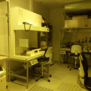
Clean Room Area
Our group-owned 60 square meter clean room area with work stations of class 100 allows for fabrication of different waveguides and photonic devices. Available equipment includes thermal, e-beam and sputter evaporators, reactive ion etching (RIE), ultra-precise dicing of different materials, optical lithography below one micron resolution, laser beam writing, spin-coating, or fine polishing. A new sputtering machine allows the fabrication of state-of-the-art dielectric mirrors for various applications.

Dicing of Ridge Waveguides
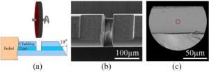
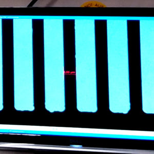
Recently optical grade dicing was introduced as a new approach to fabricate ridge waveguides in different optical materials. For this a circular precision saw is used to cut ridges into a planar waveguide. In a first step, a planar waveguide is formed using methods like ion in-diffusion, ion exchange, implantation of ions or different epitaxial methods. Remaining propagation losses of such ridge waveguides can be as low as 0.1 dB/cm, which is mainly due to the very low surface roughness of the diced sidewalls.
Publications:
M. Medina, C. E. Rüter, M. C. Pujol, D. Kip, J. Masons, A. Ródenas, M. Aguiló and F. Díaz, „KLu(WO4)2/SiO2 tapered waveguide platform for sensing applications,“ Micromachines 10, 454 (2019)
Three-Side Diffusion into LiNbO3 Ridges
In order to improve the spatial overlap of different modes inside a LiNbO3 waveguide (for example for DFG when mixing 1064 nm and 1550 nm to generate mid-infrared light around 3.4 µm), we developed a new method that uses diffusion of metals from all three side walls of a fabricated ridge. In this way overlap factors of different modes can be increased to nearly 100%.
Periodically-Poled Waveguides in Lithium Niobate (PPLN)
For efficient nonlinear frequency mixing, such as second harmonic or difference frequency generation (DFG), periodically poled lithium niobate (PPLN) is a favourite material. To allow for high intensities and thus high conversion efficiencies, waveguide geometries with cross-sections of the order of (60-80) µm² are used, where annealed proton exchange (PE) or Ti in-diffusion are the common fabrication techniques.
We do electric-field poling of e.g. planar waveguides in lithium niobate formed by either Ti in-diffusion or PE with periods ranging from 6-30 µm. Ridge waveguides diced into these substrates allow for low cross-sections as well as high overlap of the interacting modes of different wavelengths.
Publications:
S. Suntsov, D. Brüske, C. E. Rüter and D. Kip, „Watt-level 775 nm SHG with 70% conversion efficiency and 97% pump depletion in annealed/reverse proton exchanged diced PPLN ridges waveguides,“ Opt. Express 29, 11386 (2021)
Ridge Waveguides in KTP
Potassium titanyl phosphate (KTP, KTiOPO4) is a crystalline material that possess favorable optical linear and nonlinear properties and is therefore widely applied, e.g. in optical modulators or optical frequency conversion devices. It seems also attractive as a photon source for quantum cryptography applications. Waveguides in general allow to guide light and integrate multiple optical components on a single substrate. In contrast to free-space optics, light can be kept tightly confined over a long distance and this increases efficiency in nonlinear-optical processes.
We have developed a new process for the fabrication of ridge waveguide in KTP. The ridges have a typical cross section of 10×10µm², a length of 1cm and are defined by use of a diamond-blade dicing saw. The refractive index is increased homogenously within the waveguide cross-section. This is achieved by exchange of potassium (K) for rubidium (RB) ions, when the sample is immersed into a nitrate salt melt. Compared to conventional channel waveguides, these ridge waveguides profit from the ridge geometry and allow for a better overlap between modes of different wavelengths. Hence efficiency in nonlinear frequency conversion processes is improved. The waveguides have low propagation losses ≤0.4dB/cm at 1064nm. Further, they can withstand elevated temperatures without further diffusion of the Rb ions into the depth. This is due to the fact that the crystallographic z-axis is oriented horizontally and the Rb ions are only mobile along this axis.
Publications:
M. F. Volk, C. E. Rüter, M. Santandrea, C. Eigner, L. Padberg, H. Herrmann, C. Silberhorn and D. Kip, „Fabrication of low-loss Rb-exchanged ridge waveguides in z-cut KTiOPO4,“ Opt. Mater. Express 8, 82 (2018)
C. Eigner, M. Santandrea, L. Padberg, M. F. Volk, C. E. Rüter, H. Herrmann, D. Kip and C. Silberhorn, „Periodically poled ridge waveguides in KTP for second harmonic generation in the UV regime,“ Opt. Express 26, 28827 (2018)
M. F. Volk, C. E. Rüter and D. Kip, „Rb/Ba side-diffused ridge waveguides in KTP,“ Opt. Express 25, 19872-19877 (2017)
C. Chen, C. E. Rüter, M. F. Volk, C. Chen, Z. Shang, Q. M. Lu, S. Akhmadaliev, S. Zhou, F. Chen and D. Kip, „Second harmonic generation of diamond-blade diced KTiOPO4 ridge waveguides,“ Opt. Express 24, 16434-16439 (2016)
Lamellar Gratings in Silicon for Attosecond Interferometry
In our group we have designed and manufactured ultra-precise lamellar gratings used in the soft x-ray interferometer developed at DESY. These gratings are formed in single crystalline Si using ultra-precise diamond-blade dicing. Using such mirror pairs, we have recently demonstrated attosecond phase control of free-electron laser (FEL) light by generating two phase-locked replicas of x-ray pulses and observing their interference using the smart mirror as a beamsplitter. This allows for soft x-ray pump-probe experiments in the attosesond regime for, e.g., understanding the complex functionality of chemical bond formation. Soft x-ray interferometry requires high surface quality and position control of the smart mirror optics on the sub-wavelength length scale.
Publications:
S. Usenko, A. Przystawik, M. A. Jakob, L. L. Lazzarino, G. Brenner, S. Toleikis, C. Haunhorst, D. Kip and T. Laarmann, „Attosecond interferometry with self-amplified spontaneous emission of a free-electron laser,“ Nature Commun. 8, 15626 (2017)
S. Usenko, A. Przystawik, L. L. Lazzarino, M. A. Jakob, F. Jacobs, C. Becker, C. Haunhorst, D. Kip and T. Laarmann, „Split-and-delay unit for FEL interferometry in the XUV spectral range,“ Appl. Sci. 7, 544 (2017)
L. L. Lazzarino, M. M. Kazemi, C. Haunhorst, C. Becker, S. Hartwell, M. A. Jakob, A. Przystawik, S. Usenko, D. Kip, I. Hartl and T. Laarmann, „Shaping femtosecond laser pulses at short wavelength with grazing-incidence optics,“ Opt. Express 27, 13479 (2019)
S. Usenko, D. Schwickert, A. Przystawik, K. Baev, I. Baev, M. Braune, L. Bocklage, M. K. Czwalinna, S. Deinert, S. Duesterer, A. Hans, G. Hartmann, C. Haunhorst, M. Kuhlmann, S. Palutke, R. Roehlsberger, J. Roensch-Schulenburg, P. Schmidt, S. Skruszewicz, S. Toleikis, J. Viefhaus, M. Martins, A. Knie, D. Kip and T. Laarmann, „Auger electron wave packet interferometry on extreme timescales with coherent soft x-rays,“ J. Phys. B 53, 244008 (2020)
S. Skruszewicz, A. Przystawik, D. Schwickert, M. Sumfleth, M. Namboodiri, V. Hilbert, R. Klas, P. Gierschke, V. Schuster, A. Vorobiov, C. Haunhorst, D. Kip, J. Limpert, J. Rothhardt and T. Laarmann, „Table-top interferometry on extreme time and wavelength scales,“ Opt. Express 29, 40333 (2021)
S. Hartwell, A. Azima, C. Haunhorst, M. Kazemi, M. Namboodiri, A. Przystawik, D. Schwickert, S. Skruszewicz, D. Kip, M. Drescher, T. Laarmann, „Full characterization of a phase-locked DUV double pulse generated in an all-reflective shaping setup working under grazing incidence in a broad spectral range,“ Appl. Phys. B 128, 2 (2022)
D. Schwickert, M. Ruberti, P. Kolorenč, S. Usenko, A. Przystawik, K. Baev, I. Baev, M. Braune, L. Bocklage, M. K. Czwalinna, S. Deinert, S. Düsterer, A. Hans, G. Hartmann, C. Haunhorst, M. Kuhlmann, S. Palutke, R. Röhlsberger, J. Rönsch-Schulenburg, P. Schmidt, S. Toleikis, J. Viefhaus, M. Martins, A. Knie, D. Kip, V. Averbukh, J. P. Marangos, and T. Laarmann, „Electronic quantum coherence in glycine molecules probed with ultrashort x-ray pulses in real time,“ Science Advances 8, 6848 (2022)
Fiber-Optic Sensors
Fiber-optic sensors are playing an increasingly important role in diverse applications such as environmental and industrial process monitoring, chemistry, biology, and medicine. For the measurement of various physical parameters, such as refractive index, temperature, pressure or strain, a number of sensing fiber elements are used including Fabry-Pérot and Mach-Zehnder interferometer cavities, fiber Bragg and long period gratings, photonic crystal fibers and various configurations utilizing surface plasmon resonances.
Diamond blade dicing allows for easy and cost-effective fabrication of several types of sensors in a conventional single-mode step-index fiber, as well as in other fiber types, e.g. photonic crystal or multimode fibers. Using this powerful technique, we fabricated high-quality, a few tens to few hundreds micrometers long Fabry-Pérot resonator cavities by single-step cutting through the fiber core.
On the other hand, using the reduced dicing depth to partially remove only the cladding without touching the fiber core, evanescent-field-type sensors can be formed.
Recently we used optical-grade dicing to explore the concept of a “lab-in-a-needle” realized in an optical fiber. In this project, we concentrate on theoretical and experimental studies of a new sensor concept, namely the multiplexing of several, closely spaced sensors of various types at the tip of a single fiber – a topic that has been hardly investigated up to now.
The development of such fiber needle-based devices with unprecedented functionalities, high integration and small size, would allow for accurate real-time monitoring of several relevant parameters, even directly inside biological objects.
Publications:
S. Suntsov, C. E. Rüter, T. Schipkowski and D. Kip, „Fiber-integrated refractive index sensor based on a diced Fabry-Perot micro-resonator,“ Appl. Opt. 56, 9139 (2017)
S. Suntsov, C. E. Rüter and D. Kip, „Dual parameter fiber-integrated sensor for refractive index and temperature measurement based on Fabry-Perot micro-resonators,“ Appl. Opt. 58, 2076 (2019)
I. Pfalzgraf, S. Suntsov and D. Kip, „Fiber-optic sensor measuring spatial distributions of refractive index and temperature,“ Appl. Opt. 60, 1428 (2021)
Y. C. Yao, Y. R Xie, N. K. Chen, I. Pfalzgraf, S. Suntsov, D. Kip and Y. Y. Ren, „Design of fiber-tip refractive index sensor based on resonant waveguide grating with enhanced peak intensity,“ Appl. Sci. 11, 6737 (2021)
I. Pfalzgraf, S. Suntsov and D. Kip, „Multiplexing temperature-compensated open-cavity Fabry-Pérot sensors at a fiber tip,“ Appl. Opt. 60, 10402 (2021)
LNOI – Wafer Bonding of Lithium Niobate
Recently a new technology to fabricate lithium-niobate-on-insulator (LNOI) has been developed. In analogy to silicon-on-insulator (SOI), this new material platform for integrated optics enables the fabrication of optical waveguides with very small cross-sections and small bending radii due to the high refractive index contrast. As a consequence, ultra-compact photonic integrated devices such as ring resonators or nonlinear frequency mixing with superior conversion efficiency are within reach.
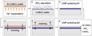
Fabrication of LNOI substrates is performed in our group in several steps. First, LiNbO3 wafers are implanted with He ions of 350 keV at a high dose. On the lower z-cut LiNbO3 substrate an optical barrier made of SiO2 is formed using e-beam evaporation. After chemical-mechanical polishing (CMP) of the SiO2 layer pre-bonding of the two wafers is achieved. Annealing to temperatures above >200°C leads to cracking of the He ion implanted layer (“smart cut”) – the LNOI material is formed.
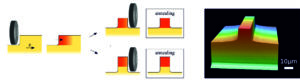
Ridges of different width [(1 – 10) microns, see picture on the upper left] can be fabricated on these LNOI substrates (LN thickness of 960 nm) using precision diamond-blade dicing which results in smooth side walls of the fabricated waveguides and low optical loss. Under optimal conditions damping values below 1dB/cm are possible.
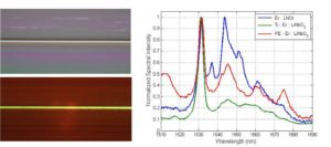
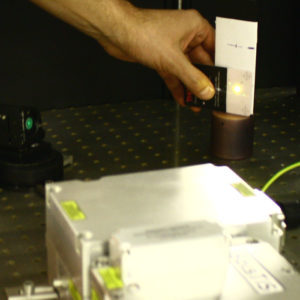
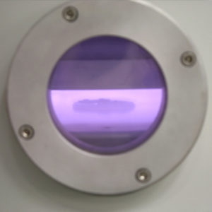
For the realization of rare earth doped integrated lasers in LiNbO3, Er-doped LNOI offers almost perfect overlap of the optical waveguide mode with the Er diffusion profile. We formed ridge waveguides in Er-doped LNOI substrates and observed strong fluorescence both in the green (lower left image, ridge pumped using 980 nm) and in the 1545 nm wavelength band (see spectrum on the right).
Publications:
M. F. Volk, S. Suntsov, C. E. Rüter and D. Kip, „Low-loss ridge waveguides in lithium niobate thin films by optical grade diamond blade dicing,“ Opt. Express 24, 1386-1391 (2016)
C. E. Rüter, D. Brüske, S. Suntsov and D. Kip, „Investigation of ytterbium incorporation in lithium niobate for active waveguide devices,“ Appl. Sci. 10, 2189 (2020)
C. E. Rüter, K. Hasse, F. Chen, and, D. Kip, „Optical characterization of neodymium-doped lithium-niobate-on-insulator (LNOI),“
Opt. Mater. Express 11, 4007 (2021).
Waveguide Lasers
We are developing integrated very compact waveguide lasers in different host materials, including YAG and lithium niobate (LiNbO3). In the last decade, there was a growing interest in the development of ridge waveguides. Compared to their channel waveguid based counterparts, ridge waveguide integrated photonic devices, such as Er:LiNbO3 waveguide amplifiers and lasers, benefit from smaller mode fields and improved overlap of modes at different wavelengths. Furthermore, in regard to the development of Er-doped Ti in-diffused LiNbO3 optical amplifiers and lasers, a ridge geometry can be used to achieve higher Er concentrations and optimized Er diffusion profiles.
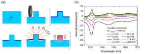
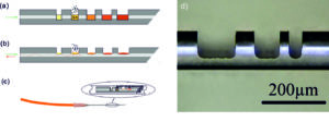
(a) Flow diagram of Er:Ti:LiNbO3 ridge waveguide fabrication. (b) Signal absorption/gain spectra at various coupled pump power levels (λpump = 1486 nm) measured for a 6 µm wide and 4.6 cm long Er:Ti:LiNbO3 ridge waveguide.
As an example, we have developed highly efficient x-cut (y-propagation) Er:Ti:LiNbO3 ridge waveguides and lasers pumped at 1486 nm using a novel fabrication technique. Ridge waveguide fabrication is comprised of ridge definition by diamond blade dicing followed by three-side Er and Ti in-diffusion, which improves the amplifier performance by allowing for higher Er concentrations and better overlap of Er diffusion profiles with the guided modes. In particular, the Er diffusion profiles were optimized for the best optical amplification by changing the relative thicknesses of Er-layers on the three ridge sides. An improved total internal small-signal gain of 14 dB at 1531 nm has been achieved in 4.6 cm-long ridge waveguides for a coupled pump power of 200 mW at 1486 nm. Utilizing this high gain efficient lasing in the third telecommunication window around 1.55 µm was realized. We demonstrated efficient Er:Ti:LiNbO3 ridge waveguide lasers operating at 1531 nm and 1561 nm with slope efficiencies of 19 % and 33 %, respectively.
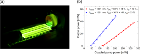
(a) Er:Ti:LiNbO3 ridge waveguide laser pumped at 1486 nm. (b) Laser output power at 1531 nm and 1561 nm versus the coupled pump power.
We are currently investigating the amplifier and laser performance of Yb-coped Er:Ti:LiNbO3 ridge waveguides pumped at 980 nm and 1486 nm. Furthermore, we will also develop efficient Nd- and Tm-doped Ti:LiNbO3 ridge waveguide lasers.
Publications:
Y. C. Jia, C. E. Rüter, S. Akhmadaliev, S. Q. Zhou, F. Chen and D. Kip, „Ridge waveguide lasers in Nd:YAG crystals produced by combining swift heavy ion irradiation and precise diamond blade dicing,“ Opt. Mater. Express 3, 433 (2013)
S. Suntsov, C. E. Rüter and D. Kip, “Er:Ti:LiNbO3 ridge waveguide optical amplifiers by optical grade dicing and three-side Er and Ti in-diffusion,” Appl. Phys. B. 123, 118 (2017)
D. Brüske, S. Suntsov, C. E. Rüter and D. Kip, “Efficient ridge waveguide amplifiers and lasers in Er-doped lithium niobate by optical grade dicing and three-side Er and Ti in-diffusion,” Opt. Express 25, 29374-29379 (2017)
S. H. Wäselmann, C. E. Rüter, D. Kip, C. Kränkel and G. Huber, „Nd: sapphire channel waveguide laser ridge waveguides,“ Opt. Mater. Express 7, 2361-2367 (2017)
D. Brüske, S. Suntsov, C. E. Rüter and D. Kip, „Efficient Nd:Ti:LiNbO₃ ridge waveguide lasers emitting around 1085 nm,“ Opt. Express 27, 8884 (2019)
K. Hasse, D. Kip and C. Kränkel, „Influence of diluted acid mixtures on selective etching of MHz- and kHz-fs-laser inscribed structures in YAG,“ Opt. Mater. Express 11, 1546 (2021)
Parity-Time Symmetric Optics
Quantum mechanics demands that each physical observable must be Hermitian. In the case of the Hamiltonian operator, this axiom not only implies real eigen-energies but also guarantees probability conservation. It is also commonly believed that hermiticity is an absolute must in order to have real eigenvalues. Interestingly however, a wide class of non-Hermitian Hamiltonians can still exhibit entirely real spectra. Among these, are Hamiltonians respecting parity-time (PT) symmetry [1]. In general, such parity-time reflection requires that the associated complex potentials obey the condition V(x)=V*(-x). Recently, it has been realized that optics can provide a fertile ground where related notions can be implemented and experimentally investigated [2-4].
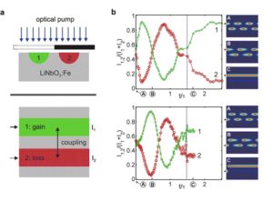
In 2010 we reported the first experimental observation of PT symmetry in an optical coupled system [5]. Such PT „optical potentials“ can be realized through a judicious inclusion of index guiding and gain/loss regions. Given that the complex refractive index distribution n(x)=n'(x)+in“(x) plays the role of an optical potential, one can then design a PT-symmetric system where the refractive index profile must be an even function of position x while the gain/loss distribution should be odd.
In our experiments we used two Ti in-diffused parallel waveguide channels in Fe-doped LiNbO3. One of the two channels was optically pumped from the top via photorefractive two-wave mixing to provide the necessary gain for the guided light, while the other neighbouring arm experienced loss. In this single-cell PT system, we observed both, spontaneous PT symmetry breaking as well as power oscillations violating left-right symmetry [5]. At t=0 the system starts to evolve from zero gain and shows a reciprocal response. However, as the photorefractive gain builds up for recording times t>0, optical wave propagation becomes strongly non-reciprocal. At the threshold, the system’s super-modes become degenerate. From thereon, power in the gain channel monotonically increases, while power in the loss channels decays.Our results, when extended to transversely periodic media (photonic lattices, waveguide arrays), pave the way towards a new class of PT-synthetic optical materials with intriguing and unexpected properties that rely on non-reciprocal light propagation and tailored transverse energy flow.
Publications:
C. E. Rüter, K. G. Makris, R. El-Ganainy, D. N. Christodoulides, M. Segev and D. Kip, „Observation of parity-time symmetry in optics,“ Nature Physics 6, 192 (2010)
K. Li, P. G. Kevrekidis, D. J. Frantzeskakis, C. E. Rüter and D. Kip, „Revisiting the PT-symmetric trimer: bifurcations, ghost states and associated dynamics,“ J. Phys. A: Math. Theor. 46, 375304 (2013)
Photonic Crystals and Waveguide Arrays
Photonic crystals are dielectric materials with periodic structuring of the optical material properties; in most cases, this is refractive index. The lattice constants are of the order of the optical wavelength. Similar to electron waves in solids (e.g., semiconductors), such photonic crystals exhibit a band structure: the propagation of optical waves is limited to certain areas – called optical bands. Between these bands, band gaps occur, in which light is not capable of propagation, but is completely reflected by the crystal. This is, among other things, the cause of the brilliant colors of „natural“ photonic crystals, as they occur, for example, in butterfly wings.
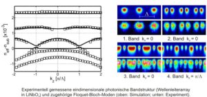
Photonic crystals offer a huge application potential e.g. in optical communications and integrated optics. Examples are miniaturized optical waveguides, devices that allow for 90-degree propagation of light, narrow-band optical filters and resonators, or even optical delay paths using extremely „slow“ light. In our group, we produce one-dimensional photonic crystals (optical waveguide arrays) in the material lithium niobate. Here, our work aims in particular at the non-linear properties of such components.
Publications:
P. G. Kevrekidis, R. L. Horne, N. Whitaker, Q. E. Hoq and D. Kip, „Bright discrete solitons in spatially modulated DNLS systems,“ J. Phys. A: Math. Theor. 48, 345201 (2015)
D. Law, J. D’Ambroise, P. G. Kevrekidis and D. Kip, „Asymmetric wave propagation through saturable nonlinear oligomers,“ Photonics 1, 390 (2014)
P. P. Belicev, I. Ilic, M. Stepic, L. Hadzievski, C. Lou, S. Suntsov, C. E. Rüter and D. Kip, „Spontaneous symmetry breaking of gap solitons in defect loaded uniform one-dimensional photonic lattices,“ Phys. Rev. A 88, 023858 (2013)
Y. Pei, Y. Hu, P. Zhang, C. Zhang, C. Lou, C. E. Rüter, D. Kip, D. N. Christodoulides, Z. Chen and J. Xu, „Coherent propulsion with negative-mass fields in a photonic lattice,“ Opt. Lett. 44, 5949-5952 (2019)
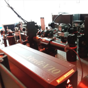
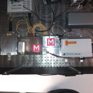
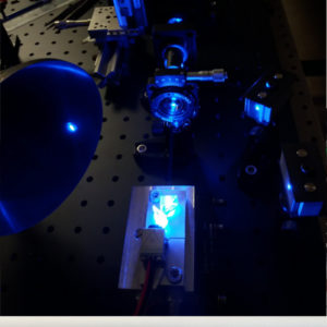
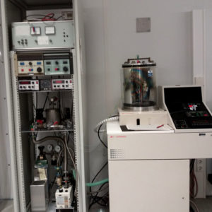
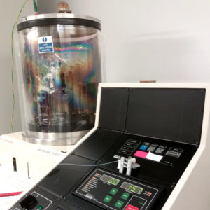
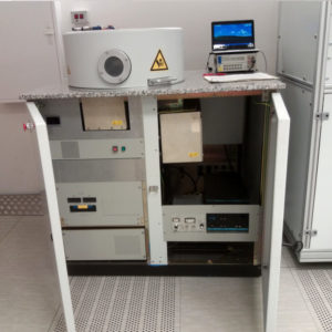
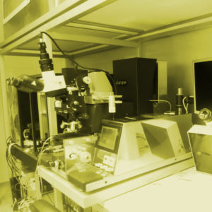
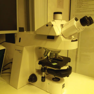
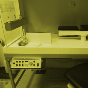
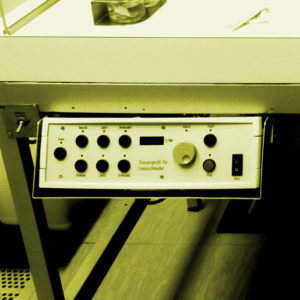
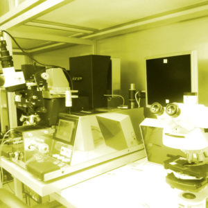
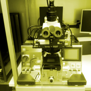
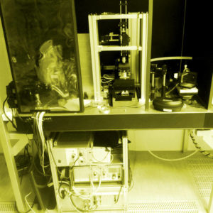
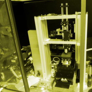
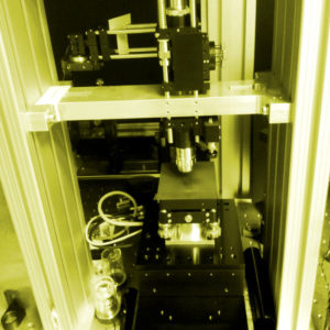
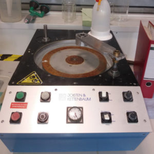
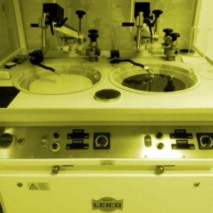
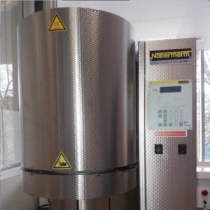
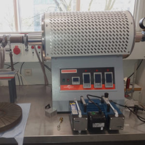
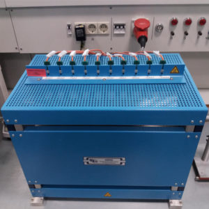
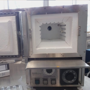
Technical Equipment
Several fully equipped laser labs of laser class 4
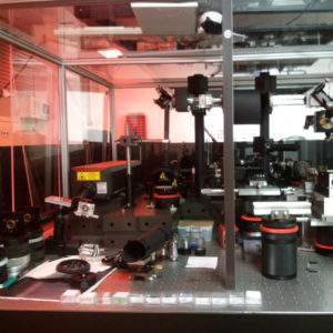
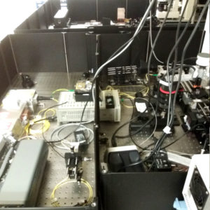
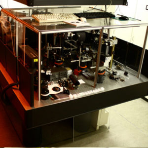
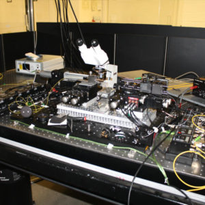
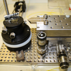
Fully automated fiber coupling setups
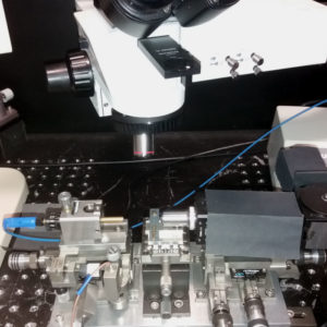
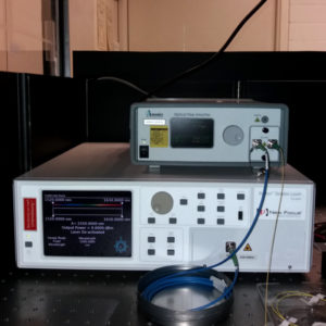
Laser sources ranging from UV to MIR

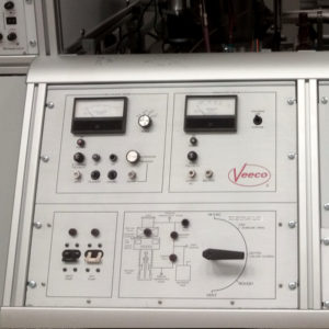
Electron beam evaporator (Veeco)
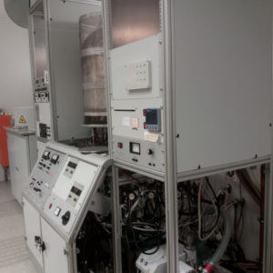
Sputter system (Edwards Auto 306)
Reactive ion etching (RIE)
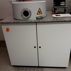
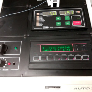
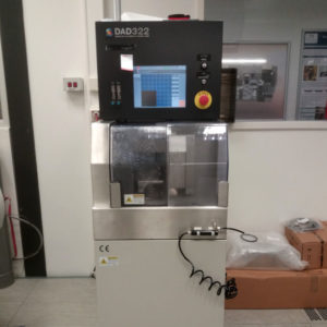
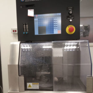
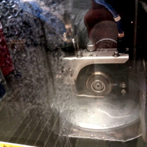
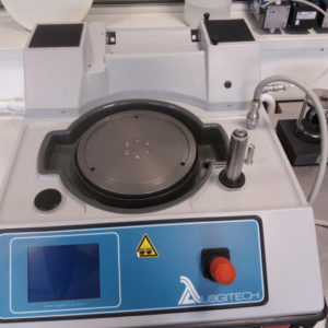
Ultra precise wafer dicing saw (Disco D322)
Clean room area with working areas of categroy class 10

Spincoater
Mask aligner (Suss MJB5)
Laser beam writing for structures down to 1 micron
X-ray spectrometer
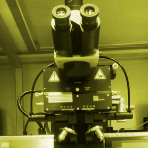
Optical microscope (Zeiss Axioplan)
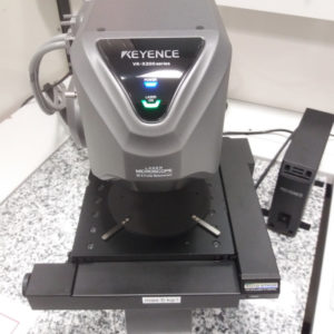
Confocal laser microscope (Keyence VK-X)
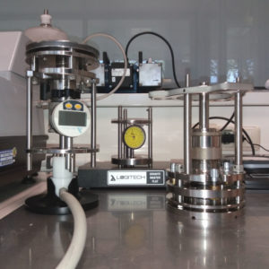
several optical polishing machines
different diffusion ovens for temperatures up to 1600°C
Letzte Änderung: 28. Juni 2022